- 您现在的位置:买卖IC网 > Sheet目录362800 > EVAL-AD1958EB (Analog Devices, Inc.) PLL/Multibit DAC
REV. 0
AD1958
–7–
CLATCH
CCLK
CDATA
D0
D15
D14
Figure 1. Format of SPI Signal
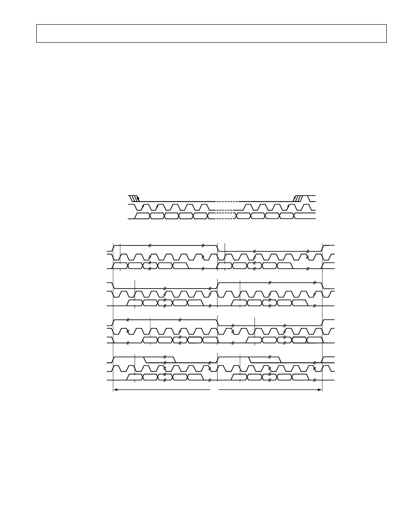
LRCLK
BCLK
SDATA
LEFT CHANNEL
RIGHT CHANNEL
MSB
MSB
MSB
MSB
MSB
MSB
LSB
LSB
LSB
LSB
LSB
MSB
MSB
LSB
LSB
LEFT-JUSTIFIED MODE—16 TO 24 BITS PER CHANNEL
1
2
S MODE—16 TO 24 BITS PER CHANNEL
RIGHT-JUSTIFIED MODE—SELECT NUMBER OF BITS PER CHANNEL
DSP MODE—16 TO 24 BITS PER CHANNEL
1/f
S
NOTES
1. DSP MODE DOES NOT IDENTIFY CHANNEL.
2. LRCLK NORMALLY OPERATES AT f
S
EXCEPT FOR DSP MODE WHICH IS 2
f
.
3. BCLK FREQUENCY IS NORMALLY 64
LRCLK BUT MAY BE OPERATED IN BURST MODE.
LRCLK
BCLK
SDATA
LRCLK
BCLK
SDATA
LRCLK
BCLK
SDATA
LEFT CHANNEL
RIGHT CHANNEL
LEFT CHANNEL
RIGHT CHANNEL
LSB
Figure 2. Stereo Serial Modes
The SPI control port is a 3-wire serial control port. The format
is similar to the Motorola SPI format except the input data word
is 16 bits wide. Max serial bit clock frequency is 8 MHz and
may be completely asynchronous to the PLL system or the
DAC. Figure 1 shows the format of the SPI signal. Note that
the CCLK can be gated or continuous,
CLATCH
should be
low during the 16 active clocks.
POWER SUPPLY AND VOLTAGE REFERENCE
The AD1958 is designed for five-volt supplies. Separate power
supply pins are provided for the analog, digital, and PLL sec-
tions.
These pins should be bypassed with 100 nF ceramic
chip capacitors, as close to the pins as possible, to minimize
noise. A bulk aluminum electrolytic capacitor of at least 22
μ
F
should also be provided on the same PC board. For best perfor-
mance it is recommended that the analog supply be separate
from the digital and PLL supply. It is recommended that all
supplies be isolated by ferrite beads in series with each supply. It
is expected that the digital and PLL sections will be run from a
common supply but isolated from one another. It is important
that the analog supply be as clean as possible.
The internal voltage reference is brought out on Pin 21 (FILTR)
and should be bypassed as close as possible to the chip with a
parallel combination of 10
μ
F and 100 nF. The reference volt-
age may be used to bias external op amps to the common-mode
voltage of the analog output signal pins. The current drawn
from the FILTR pin should be limited to less than 50
μ
A.
SERIAL DATA PORTS—DATA FORMAT
The DAC serial data input mode defaults to I
2
S. By changing
Bits 4 and 5 in the DAC control register, the mode can be
changed to RJ, DSP, or LJ. The word width defaults to 24 bits
but can be changed by programming Bits 8 and 9 in the DAC
Control Register.
Figure 2 shows the serial mode formats.
发布紧急采购,3分钟左右您将得到回复。
相关PDF资料
EVAL-AD1959EB
PLL/Multibit DAC
EVAL-AD1974EB
4 ADC with PLL, 192 kHz, 24-Bit Codec
EVAl-AD1974EBZ
4 ADC with PLL, 192 kHz, 24-Bit Codec
EVAL-AD1990EB
Audio Switching Amplifier
EVAL-AD1992EB
Audio Switching Amplifier
EVAL-AD1994EB
Audio Switching Amplifier
EVAL-AD421EB
Loop-Powered 4 mA to 20 mA DAC
Eval-AD5025EBZ
Fully Accurate 12-/14-/16-Bit VOUT DAC SPI Interface 2.7 V to 5.5 V in a TSSOP
相关代理商/技术参数
EVAL-AD1959EB
制造商:AD 制造商全称:Analog Devices 功能描述:PLL/Multibit DAC
EVAL-AD1970EB
制造商:Analog Devices 功能描述:EVAL BD BTSC ENCODER W INTEGRATED CODEC - Bulk
EVAL-AD1974AZ
功能描述:BOARD EVAL FOR AD1974 RoHS:是 类别:编程器,开发系统 >> 评估板 - 模数转换器 (ADC) 系列:- 产品培训模块:Obsolescence Mitigation Program 标准包装:1 系列:- ADC 的数量:1 位数:12 采样率(每秒):94.4k 数据接口:USB 输入范围:±VREF/2 在以下条件下的电源(标准):- 工作温度:-40°C ~ 85°C 已用 IC / 零件:MAX11645 已供物品:板,软件
EVAL-AD1974EB
制造商:AD 制造商全称:Analog Devices 功能描述:4 ADC with PLL, 192 kHz, 24-Bit Codec
EVAL-AD1974EBZ
制造商:Analog Devices 功能描述:EVAL KIT FOR 4 ADC W/ PLL, 192 KHZ, 24BIT CODEC EVAL-AD1974E - Boxed Product (Development Kits)
EVAL-AD1990EB
制造商:Analog Devices 功能描述:EVAL BD CLASS D AUDIO POWER OUTPUT STAGE - Bulk
EVAL-AD1992EB
制造商:AD 制造商全称:Analog Devices 功能描述:Audio Switching Amplifier
EVAL-AD1994EB
制造商:Analog Devices 功能描述:EVAL BOARD FOR AD1994 - Bulk